One woman and her quest to implement a binary down counter in hardwired logic for .. fun?
Introduction
I posted the above video of a 4-Bit Down Counter, with 7 segment decimal display on [redacted social media site], and had comments expressing interest in how this circuit worked.
Luckely, I had already written a detailed description of the design process for marked coursework. Which means that this blog post is almost entirely copied verbatium from this coursework, expect it to be informative and dry.
This type of circuit design may seem archaic with the advent of cheap and easily accessible microcontrollers, but this kind of pure logic excercise is still applicable to modern electronics.
Look into the very high speed and reliable signal processing equipment that we rely on to encode and decode video in almost realtime, fly planes, run automation and you will find FPGAs, Field Programmable Gate Arrays. Operations done by physical logic circuits are faster, more repeatable and easier to certify than microcontrollers running firmware. When we program an FPGA, we are creating a physical logic circuit to do a task, rather than running a program on a controller.
With all that said, lets get to the actual task we have set ourselves for this project. Counting down from 9 to 0.
This project is split into two halves:
- 4-bit Down Counter: This is a sequential logic circuit, its state is dependent on the previous state.
- 7-Segment Display Driver This is a combinational logic circuit. Its output is only dependent on the current input.
Both circuits are solved in almost exactly the same way, so this first post will cover the entire design and construction of the sequential circuit, and the next post will be regarding the combinational logic circuit.
Sequential Logic Circuit -Decade Down Counter
This project is aimed at designing, modelling, building and testing, a decade down counter with a 7 segment display. The 7 segment display will use a combinational logic circuit to translate a binary 4-bit value into the output display, while the sequential logic circuit will be a 4-bit binary down counter using D-Type latches. This report will focus on the 4-bit binary down counter.
Theory & Background
In order for a circuit to act sequentially, it must have some kind of feedback from the output to some point in the circuit. This feedback is often achieved with the use of latching circuits, which can “save” a particular state at a moment of time, and this state feeds back to the inputs of the logic network. This is the principle behind computer memory. Sequential circuits can also be of one of two types, asynchronous or “ripple”, where a clock source is fed to just the first of the latching circuits, and the output from this latch acts as the clock for the next latch in the circuit, or they can be synchronous, where the clock source is fed to each of the latching circuits and so the state of the system is updated with each clock cycle. In the case of this circuit, it will be designed to be synchronous, as this is less likely to output errors or be subject to “race conditions” where some part of the circuit is not yet in the expected state due to propagation delay.
Designing the State Machine
The first step to designing a sequential logic circuit, is to draw a diagram of the required states. In this case the task is to count from 9, down to 0, then return to 9 in binary. Therefore a state flow diagram was created, which shows the binary state along with the decimal equivalent.
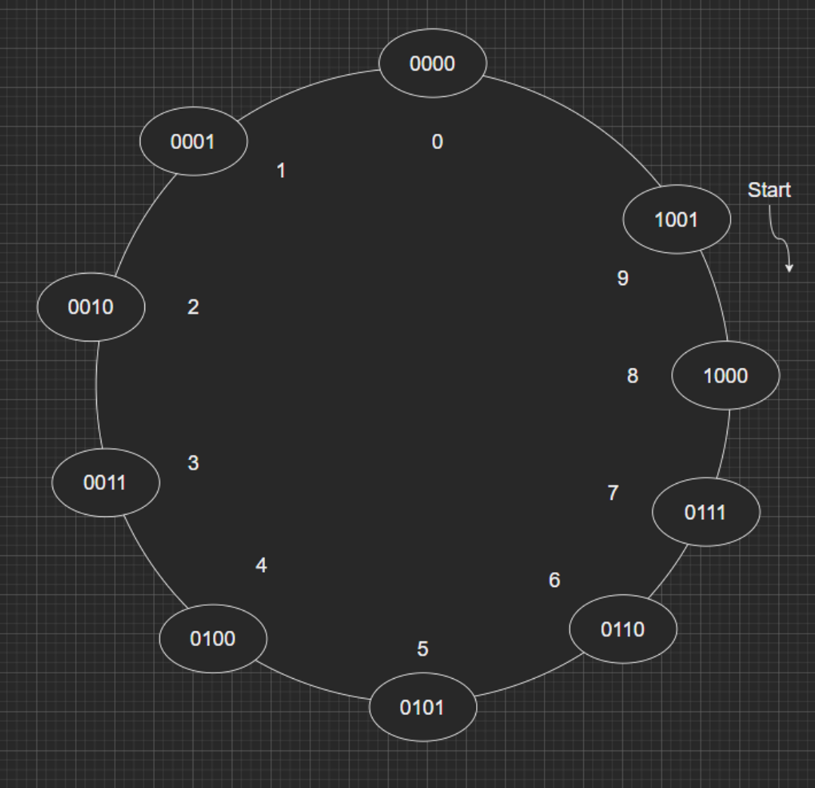
With the state flow defined, the next step is to decide which latching or flip-flop circuit to use. Use of a latching circuit enables the circuit to have both memory, and a clock input which can synchronise the circuit to change state at a single point in time.
Creating a Characteristics Table
In this case D-type latches were selected as they were available. A characteristics table shows what the next output state Q(n+1) would be given the state of the input (D) and the current state of the output (Qn).
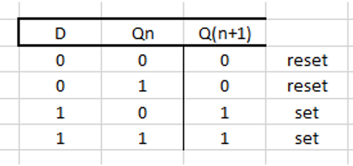
In this diagram it should be clear that the current state (Qn) does not have an impact on the following state, as the output is latched to whatever the input state (D) is at the time of the positive clock pulse. The characteristics table for the latches selected can be used to generate an excitation table.
Creating an Excitation Table
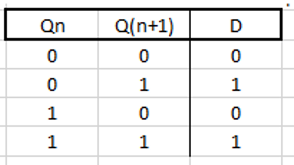
This shows what input (D) would be required to produce a specific state Q(n+1), given the current state (Qn).
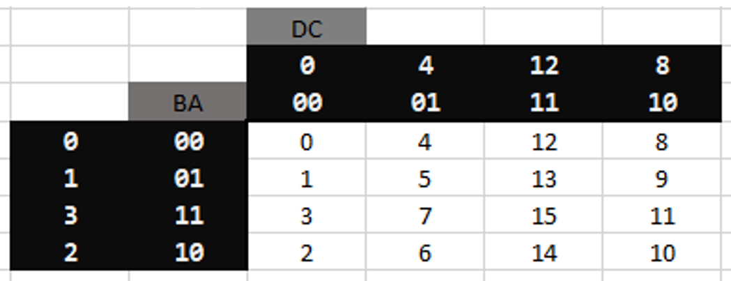
Now an excitation table can be completed for the entire circuit. This will show the current state of each input, the desired next state (using the state flow diagram created earlier) and the input required to generate the next state.
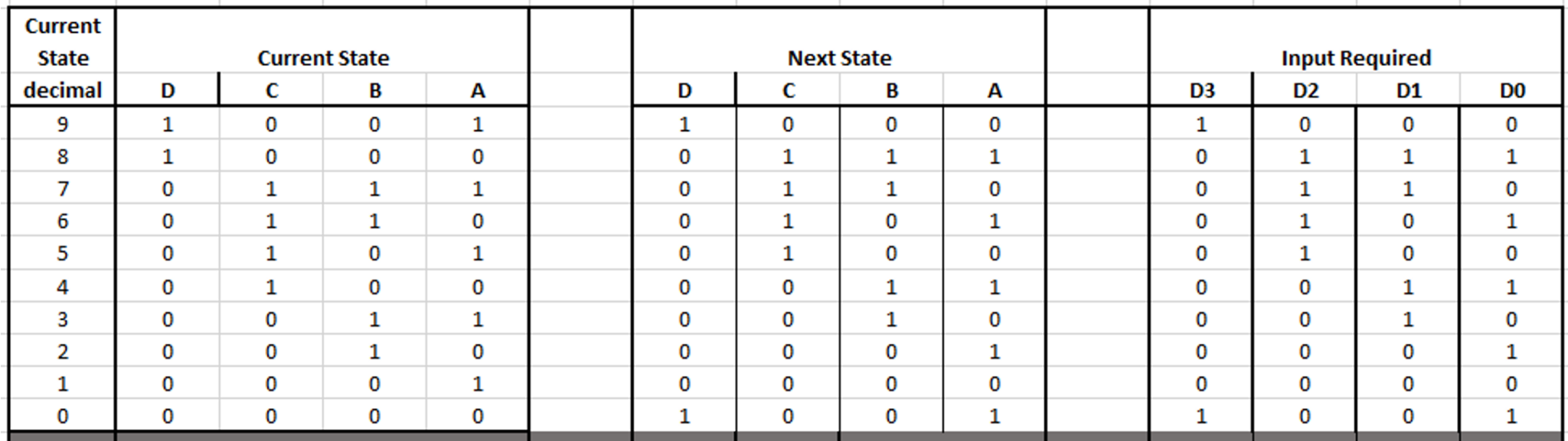
The last state in the current state table, 0 or (0,0,0,0) if each individual bit is considered, must then go back to state 9 or (1,0,01), this is shown on the next state table. As D-type latches were selected, the input required to generate the next state is the same as the next state. This means that D = Q(n+1). However if different latch circuits were specified then the input required table might not conform in this way. This is why the excitation table is important, as it shows the input required to obtain a specific outcome, given the current state. Now Karnaugh maps (K-Maps) for each of the input bits (D_0,D_1,D_2,D_3) can be generated.
Developing Karnaugh Maps (K-Maps)
Now is where the real magic begins!
In a Karnaugh map, or K-Map, the input bits are arranged along the X and Y axis, following grey code implementation. This is to ensure that only one bit changes at a time as one moves across or down the axis. This remains true for cells that loop around from the end of one axis back to the start. It is not necessary, however it is advantageous to fill in the decimal number created in each cell as a combination of the bits on both the X and the Y axis.
K-Map for D_0
The next step of the process is to highlight all the cells that are true for each bit in turn. First a k-map for the first latch D_0, representing the least significant bit in the binary number, was created using the column from the input required section of the table and the decimal value of the current state. (Note, it is possible to just use the state of each bit, however it saves time when filling in the k-map to use the decimal values).
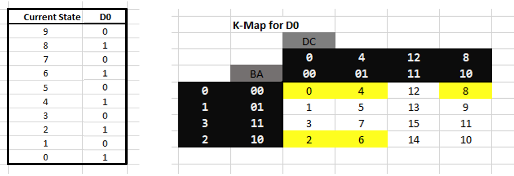
Using this section of table, it is possible to see that D_0 must be true for states: 8, 6, 4, 2, and 0. Therefore these cells are highlighted in yellow in the k-map table. Groups can now be formed using the highlighted cells. Each group must contain 2^n cells, with the smallest group being a single cell. A group cannot contain any white cells. Groups can wrap around from the end of an axis to the start of the axis. Following these rules, the 4 corners could be a valid group if they are all highlighted cells. To find the simplest expression, the number of groups should be minimised, while the size of each group is maximised. Cells can be included in more than one group, and every highlighted cell must be included in at least 1 group. All groups must be rectangular.

In this case the largest groups that can be formed of highlighted cells are shown in the above diagram. As there are two groups, the expression will be two ANDed groups ORed together. To derive the Boolean expression, the bits that do not change are noted down. Starting with the pink group, the A bit is FALSE and does not change, so the expression will contain a NOT A, or ¯A. The B bit does change, so is excluded, the C-bit also changes state and so is excluded, and the D-bit is FALSE and does not change, so the expression for this group is ¯A ¯D. The blue group contains only 2 cells, A and B are both false and do not change, the C bit is also false and does not change, and the D bit does change state, therefore the expression for this group is ¯A ¯B ¯C or: ((not A) AND (not B) AND (not C)) These expressions are ORed together, therefore the Boolean expression for this k-map is: D_0= ¯A ¯D + ¯A ¯B ¯C Where + means OR. This process is followed for each of the data input bits (D_0,D_1,D_2,D_3 ), first generating a k-map, then grouping cells and deriving the Boolean expression. Please find the completed k-maps, with highlighted groupings and the resultant Boolean expressions below.
K-Map for D_1

For input D_1 it is clear that it requires true for states 8, 7, 4, and 3, therefore these states are highlighted on the k-map for this input. In this case, 3 groups are able to be formed, which means that the Boolean expression that will result will be 3 ANDed expressions ORed with each other. Therefore: Blue: Single cell means that all bits are required, expression is ¯A ¯B C ¯D Green: C changes, D and BA do not, therefore the expression is A B ¯D, or (A AND B AND NOT D) Pink: All bits are required, expression is ¯A ¯B ¯C D These 3 expressions are ORed together, making the final Boolean expression for this k-map: D_1=¯A ¯B C ¯D+A B ¯D+ ¯A ¯B ¯C D The same process is followed for the remaining data inputs
K-Map for D_2

K-Map for D_3

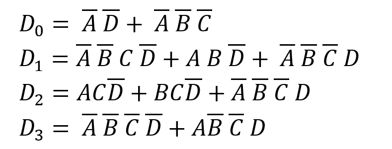
Finished Logic Expressions for Each Input
Moddeling the Logic Circut
In order to test the logic circuit, a model was created in LabVIEW, using the same logic gates that would be used in the final circuit.
Modelling a D-Latch
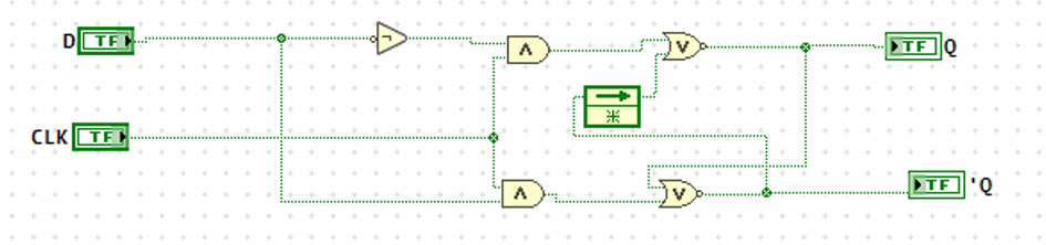
The first step to model this circuit in LabVIEW, was to make a subVI (program in LabVIEW) to replicate the action of a D-latch. This was done using logic gates and a feedforward node, to allow the feedback from the ¯Q output as an input to the NOR gate.
This subprogram was given a logo mirroring the schematic symbol for a D-latch, and was placed into the main VI for the decade down counter. 3 copies of this subVI were created to ensure that LabVIEW would use 4 different instances of the D-latch. [2] The outputs from these D-latches were tied to a Boolean cluster of 4-bits, and these clusters were passed to both a 4-bit LED indicator on the LabVIEW front panel, and to shift-registers, which allow the program to be placed into a looping structure and retain the values from the last loop. A clock input was provided to all of the D-Latches that could be triggered by pressing a momentary button on the main VI user interface. Together this replicated the function of D-latches in a sequential circuit. Finally, the shift register output was used to provide the 4 bit A, B, C, and D values to the start of the circuit, and NOT gates were used to provide the NOT of each of these inputs.

Modelling a D-Latch
The logic circuit can now be added and inputs taken as required from one of the labelled wires within the looping structure.
The logic circuit was then built, following the expressions generated above for each Data input.
Implementing the Digital Circuit Models
The logic circuit can now be added and inputs taken as required from one of the labelled wires within the looping structure. The logic circuit was then built, following the expressions generated above for each Data input.
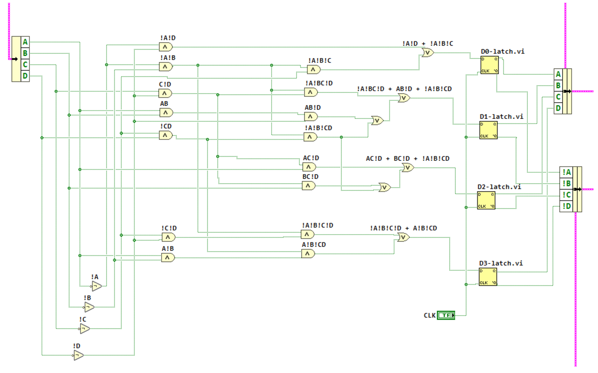
This program was run and it was confirmed that the logic circuit functioned as expected. The figure below shows the first 3 state transitions, triggered by manually clicking the CLK button.

Electronic Schematic
A schematic was drawn using the logic circuit confirmed via LabVIEW. Some mistakes were made during the initial attempt at this, and a slightly different logic circuit was captured via schematic. This schematic represents the implementation used for the physical circuit, and the changes can be accounted for due to selecting different groupings of cells when initially analysing K-Maps.

The clock input was implemented with a button, so states could be cycled through manually, though this cant eb replaced with a simple 555 timer later. The output of the circuit was shown via 4 LEDs arranged as a binary display.
Building the Circuit
Now the logic is confirmed, we are able to build the physical circuit using IC’s.

Validation
During initial testing it was found that a single switch press would often trigger several clock pulses unintentionally. In order to avoid this happening, the switch was debounced using a 10uF capacitor and a resistor. This meant that the time taken for the clock rail to increase and then decrease in voltage after a button press was increased, which helps avoid multiple triggers being detected as the contacts make and break contact several times over the course of a single button press. The circuit functioned as expected, each time the button was clicked the value shown on the binary display counted down from 9 to 0, and back to 9.
Conclusion
I hope you found this method interesting to learn about, please feel free to comment and share anything you create using this method!
Join us next time where we will calculate then build a display for this circuit to display the decimal numbers instead of just a binary output.